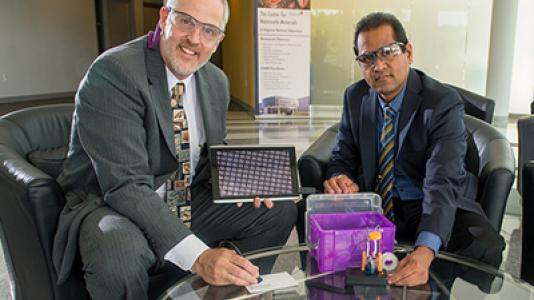
ARGONNE, Ill. — Three inventions created by researchers at the U.S. Department of Energy’s Argonne National Laboratory have received 2014 R&D 100 awards.
The awards, organized by R&D magazine, have been given out annually since 1962 for the top technologies of the year and are widely considered to be the “Oscars of Innovation.” Argonne scientists have won 123 R&D 100 awards since they were first introduced in 1964.
“These awards recognize the tremendous value of our national labs,” said Secretary of Energy Ernest Moniz. “Research and development at the national labs continues to help our nation address its energy challenges and pursue the scientific and technological innovations necessary to remain globally competitive.”
This year’s winners from Argonne include:
- Sequential Infiltration Synthesis (SIS) lithography
- Advanced Redox Shuttle Additive for Overcharge Protection of Lithium-Ion Batteries Used in Electric Vehicles
- The NanoFab Lab…in a Box!
“Once again, the ingenuity of Argonne’s scientists and engineers has been recognized by the R&D 100 awards, which highlight the most innovative and significant new technologies as they enter the marketplace,” said Argonne Director Peter B. Littlewood. “We are very proud that the work of Argonne researchers has culminated in these important inventions that promise to further advanced manufacturing of a wide range of high-tech electronics and to make state-of-the-art lithium batteries even safer.”
Sequential infiltration synthesis (SIS) lithography
Sequential infiltration synthesis (SIS) lithography is a new way of creating nanoscale patterns for microelectronics manufacturing that will reduce cost and improve product performance.
Useful for a number of different applications, including the creation of semiconducting computer chips and magnetic recording devices, lithography typically refers to the method of using light or electrons to pattern a material. These patterns are traced into a material called a “resist” and are then transferred to the corresponding regions of the underlying material, called the substrate, during further processing steps.
On their own, however, resists typically degrade quickly, especially in the presence of a number of different reactive gases during the etching process. To combat this, engineers typically use a material called a “hard mask” to protect the pattern fidelity during processing. Unfortunately, this extra step often perpetuates a part of the problem it attempts to solve, as some of the pattern resolution is lost. “The addition of the hard mask adds additional steps, creating something like a game of ‘telephone,’ with successfully more quality being lost along the way,” said Argonne scientist Seth Darling of Argonne’s Center for Nanoscale Materials, one of the award winners.
Sequential Infiltration Synthesis (SIS) is a way to eliminate the extra step of introducing the hard mask by instead growing inorganic materials directly inside the resist. “Growing hard mask material inside the original resist saves you steps, which saves you cost and improves pattern quality,” Darling said. “There can be dozens of lithographic cycles required to make a computer chip, so that’s dozens of steps you no longer need to do.”
SIS also has the potential to transform the next generation of lithographic techniques, known as block copolymer lithography. In block copolymer lithography, two different polymers self-assemble to form a resist composed of arrays of nanoscale features. This eliminates the need for light or electron beam exposure, but still necessitates that the polymers have different etch resistances – so that the pattern is still left behind – and that at least one has a high etch resistance, so it doesn’t quickly degrade.
“Both of these are challenging criteria to meet,” Darling said. “But the amazing thing is that we can perform SIS selectively in just one of the polymers but not the other, creating the differential that we’re looking for. In essence, SIS solves both of our problems at the same time.” In addition to Darling, the winning team includes Argonne scientists Jeffrey Elam, Qing Peng, Yu-Chih Tseng, David Czaplewski, Anil Mane and Leonidas Ocola.
Advanced redox shuttle additive for overcharge protection of lithium-ion batteries used in electric vehicles
Without adequate protection, overcharging a lithium-ion battery can lead to all kinds of problems, perhaps the most significant of which is the risk of a sudden increase in the voltage leads to a rapid increase in temperature in a phenomenon called “thermal runaway,” which can start fires.
In order to make sure this doesn’t happen, lithium-ion battery manufacturers have built in electronic safeguards designed to shut down overcharging before it begins. But Argonne chemists Zhengcheng (John) Zhang has developed a chemical solution to the problem as well.
Known as a redox shuttle additive, the chemical is added to the battery’s electrolyte – the material that separates the two electrodes. The redox shuttle additive prevents overcharging by electrochemically “locking in” a maximum voltage that is dependent on the chemical structure of the additive and the nature of the battery material.
“It’s an excellent backup system,” Zhang said. “Even without the electronic system, the redox shuttle additive on its own is enough to prevent overcharging.”
The redox shuttle additive also allows researchers to create an “autobalancing” battery, which refers to the thousands of different battery cells in a pack being electrochemically instructed to charge in concert.
In addition to the overcharge protection, the redox shuttle technology Argonne developed is cost-effective because of the inexpensive starting materials and simple manufacturing process, according to Zhang. “It really addresses our two major issues at the same time: cost and safety,” he said.
Different batteries charge to different voltages, so Zhang’s group created a variety of different redox shuttle additives that are each tailored for a different class of battery cathode materials. Then, Argonne chemist Greg Krumdick and his group scaled up the materials from the gram-level to the kilogram-level, making them attractive candidates for commercialization.
“This is an example of true collaboration,” Krumdick, who also won an R&D 100 award for the technology, said. “If [Zhang] didn’t invent this substance in the first place, we would have nothing to scale up, but without the scaling we wouldn’t be able to attract industry as easily.”
NanoFab lab…in a box!
The “NanoFab lab…in a box!” is a shoebox-sized mini-laboratory for growing nanowires. Nanowires are extremely thin wires on the order of 10 nanometers across (for comparison, your fingernails grow one nanometer per second). The standard technique to make them requires an expensive “clean room,” a lab with extensive filters to keep out the hundreds of thousands of particles usually floating in the air.
Nanowires are a relatively new technology, but scientists believe that they could have applications in fabricating transistors, in sensors, in solar cells and as electronic components.
The nanowires are created using an ultrananocrystalline diamond (UNCD) template, which can be used an indefinite number of times. The nanowires grow at the edge of a conducting form of UNCD that is sandwiched between an insulating UNCD layer and a silicon substrate.
The “NanoFab lab…in a box!” was a brainchild of University of Wisconsin-Stevens Point professor Michael Zach, who teamed up with Argonne nanoscientist and UNCD-specialist Ani Sumant of Argonne’s Center for Nanoscale Materials. This R&D 100 award represents the third such award Sumant has won in the past two years and his fourth overall. It is the second such award for Zach.
“Previously, scientists had to develop separate techniques to fashion different types of nanowires, but now we’ve developed a reusable template or ‘printing press’ that speeds the process from hours or days to minutes or even seconds,” Zach said.
“No one had thought that nanowires could be created so simply and inexpensively,” Sumant added. “The properties of the diamond allow us to use it like a stamp repeatedly to create essentially whatever pattern we want.”
Because the kit is both portable and inexpensive, Zach believes that the technology offers a unique opportunity for scientists to do education and outreach. “Most schools don’t have the resources to perform expensive nanotechnology experiments, but our invention allows us to bring nanotechnology to the classroom in a very tangible way.”
“This technique has great potential for producing nanowires of many different materials on a mass scale at much lower cost than any other existing methods, and is therefore attractive for many applications,” Sumant added.
Argonne National Laboratory seeks solutions to pressing national problems in science and technology. The nation’s first national laboratory, Argonne conducts leading-edge basic and applied scientific research in virtually every scientific discipline. Argonne researchers work closely with researchers from hundreds of companies, universities, and federal, state and municipal agencies to help them solve their specific problems, advance America’s scientific leadership and prepare the nation for a better future. With employees from more than 60 nations, Argonne is managed by UChicago Argonne, LLC for the U.S. Department of Energy’s Office of Science. For more visit www.anl.gov.
The Center for Nanoscale Materials at Argonne National Laboratory is one of the five DOE Nanoscale Science Research Centers (NSRCs), premier national user facilities for interdisciplinary research at the nanoscale, supported by the DOE Office of Science. Together the NSRCs comprise a suite of complementary facilities that provide researchers with state-of-the-art capabilities to fabricate, process, characterize and model nanoscale materials, and constitute the largest infrastructure investment of the National Nanotechnology Initiative. The NSRCs are located at DOE’s Argonne, Brookhaven, Lawrence Berkeley, Oak Ridge and Sandia and Los Alamos National Laboratories. For more information about the DOE NSRCs, please visit http://science.energy.gov/bes/suf/user-facilities/nanoscale-science-research-centers.