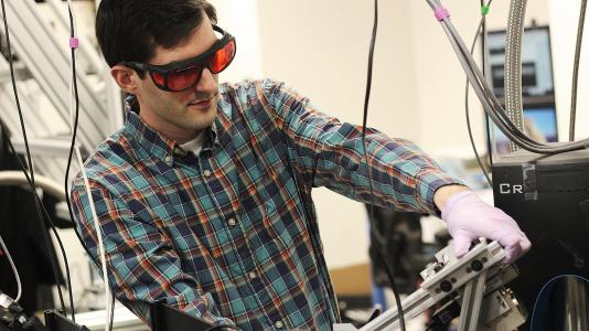
Researchers at the University of Chicago and the U.S. Department of Energy’s Argonne National Laboratory have developed a new method to measure how photocurrents flow in a 2D material — a result that could have implications for developing quantum sensors and next-generation electronics.
By using quantum sensors to visualize the magnetic field in extremely thin molybdenum disulfide (MoS2) — a material just three atoms thick — the team discovered just how photocurrents (electric currents induced by light) flowed in the material — in this case, surprisingly, in a vortex around the laser. This ultra-sensitive method of measuring such currents in a two-dimensional material, which is a substance with a thickness of a few nanometers or less, will help researchers better understand the material in the hopes of eventually using it to create flexible electronics and solar cells. The results were published on January 6 in the journal Physical Review X.
“The ability to observe electronic behavior that is invisible to traditional measurements opens new avenues for scientific study, and ultimately helps us design efficient quantum technologies,” said principal investigator David Awschalom, Liew Family Professor of Molecular Engineering, senior scientist at Argonne National Laboratory, and director of the Chicago Quantum Exchange. “This sensitive measurement technique allows us to explore phenomena at the atomic scale and develop new devices for quantum sensing and communication.
Measuring currents in extremely thin materials
To make the measurement, Awschalom and the team placed MoS2 on a nitrogen-vacancy center, which is a defect in a diamond where a nitrogen atom sits next to a vacant site in the diamond’s lattice. These spots can be used to study electronic and nuclear spin phenomena.
The team then shined a red laser onto the material to see if they could detect any temporary magnetic disturbances (that they hypothesized the laser might cause). But instead of magnetic disturbances, they detected strong photocurrents, which can result when light is shined onto a material. These photocurrents produce magnetic fields as they flow. Photocurrents are the basis behind the technology in digital cameras, solar cells, and fiber-optic networks.
The researchers were surprised to discover the photocurrents traveling in a vortex around the laser — a shape that would be impossible to detect with other techniques.
Traditional methods to measure how photocurrents flow through MoS2 are difficult to perform and are often incorrect. Understanding this phenomenon is important to develop potentially flexible and transparent electronics from MoS2 and other 2D materials.
“We are much happier that we found photocurrents instead of the magnetic disturbances we were looking for,” said Paul Jerger, a graduate student in Awschalom’s UChicago lab and at Argonne, who conducted the research with former postdoctoral fellow Brian Zhou, who is now at Boston College. “Understanding photocurrents will help us better understand the electrical properties of materials like this, with the hopes of using them for electronics like digital cameras or solar cells.”
Creating more compact quantum devices
The finding could pave the way for better experimental setups in the lab, where the nitrogen-vacancy centers are used to conduct quantum operations. It will also be useful for understanding how photocurrents are generated and propagated, which could enable researchers to use thin materials for digital cameras, solar cells, or even on-demand magnetic fields that don’t require any electrical wires.
Next the team hopes to adapt the process to measure photocurrents at room temperature, and to try to apply this technique to measure photocurrents in other thin materials, like graphene.
“As we synthesize quantum materials of the highest quality, we ideally want to measure them without making disruptive electrical connections,” said Jiwoong Park, professor of chemistry at UChicago and joint appointee at Argonne, whose group created the MoS2 used in the study. “This new technique allows us to do that, paving the way to develop novel quantum materials in industrial-scale processes.”
Other authors on the paper include Kan-Heng Lee, Masaya Fukami, and Fauzia Mujid.
This research was funded in part by the National Science Foundation, the Air Force Office of Scientific Research and the Army Research Office.
Argonne National Laboratory seeks solutions to pressing national problems in science and technology. The nation’s first national laboratory, Argonne conducts leading-edge basic and applied scientific research in virtually every scientific discipline. Argonne researchers work closely with researchers from hundreds of companies, universities, and federal, state and municipal agencies to help them solve their specific problems, advance America’s scientific leadership and prepare the nation for a better future. With employees from more than 60 nations, Argonne is managed by UChicago Argonne, LLC for the U.S. Department of Energy’s Office of Science.
The U.S. Department of Energy’s Office of Science is the single largest supporter of basic research in the physical sciences in the United States and is working to address some of the most pressing challenges of our time. For more information, visit https://energy.gov/science.