The electronics world has been dreaming for half a century of the day you can roll a TV up in a tube. Last year, Samsung even unveiled a smartphone with a curved screen—but it was solid, not flexible; the technology just hasn’t caught up yet.
But scientists got one step closer last month when researchers at the U.S. Department of Energy’s Argonne National Laboratory reported the creation of the world’s thinnest flexible, see-through 2-D thin film transistors.
These transistors are just 10 atomic layers thick—that’s about how much your fingernails grow per second.
Transistors are the basis of nearly all electronics. Their two settings—on or off—dictate the 1s and 0s of computer binary language. Thin film transistors are a particular subset of these that are typically used in screens and displays. Virtually all flat-screen TVs and smartphones are made up of thin film transistors today; they form the basis of both LEDs and LCDs (liquid crystal displays).
“This could make a transparent, nearly invisible screen,” said Andreas Roelofs, a coauthor on the paper and interim director of Argonne’s Center for Nanoscale Materials. “Imagine a normal window that doubles as a screen whenever you turn it on, for example.”
To measure how good a transistor is, you measure its on-off ratio—how completely can it turn off the current?—and a property called “field effect carrier mobility,” which measures how quickly electrons can move through the material.
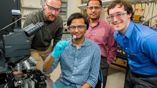
“We were pleased to find that the on/off ratio is just as good as current commercial thin-film transistors,” said Argonne postdoctoral scientist and first author Saptarshi Das, “but the mobility is a hundred times better than what’s on the market today.”
The team also tried bending the films to test what happens under stress. In most thin film transistors, the material starts to crack, which, as you might imagine, affects performance. “But in ours, the properties didn’t change at all,” Roelofs said. “The layers just slide and don’t crack.”
The transistors also maintained performance over a wide range of temperatures (from -320°F to 250°F), a useful property in electronics, which can run very hot.
To build the transistors, the team started with a trick that earned its original University of Manchester inventors the Nobel Prize: using a strip of scotch tape to peel off a sheet of tungsten diselenide just atoms thick.
“We chose tungsten diselenide because it provides the electron and hole conduction necessary for making transistors with logic gates and other p-n junction devices,” said Argonne scientist and coauthor Anirudha Sumant.
Then they used chemical deposition to grow sheets of other materials on top to build the transistor layer by layer. The final product is 10 atomic layers thick. (See sidebar for an illustration).
Next, the team is interested in adding logic and memory to flexible films, so you could make not just a screen but an entire flexible and transparent TV or computer.
“However, more work needs to be done in developing large-area synthesis of tungsten diselenide to realize the true potential for applications of our work,” said Sumant.
The study, “All Two-Dimensional, Flexible, Transparent, and Thinnest Thin Film Transistor,” was published in Nano Letters. The other author on the study was graduate student Richard Gulotty. The work is a collaborative effort between the High Energy Physics and Nanoscience and Technology divisions at Argonne, based on the idea that multi-disciplinary research projects structured to address grand science challenges could expedite technological progress for all disciplines.
The Center for Nanoscale Materials, where the work was conducted, is supported by the U.S. Department of Energy’s Office of Science.
Argonne National Laboratory seeks solutions to pressing national problems in science and technology. The nation’s first national laboratory, Argonne conducts leading-edge basic and applied scientific research in virtually every scientific discipline. Argonne researchers work closely with researchers from hundreds of companies, universities, and federal, state and municipal agencies to help them solve their specific problems, advance America’s scientific leadership and prepare the nation for a better future. With employees from more than 60 nations, Argonne is managed by UChicago Argonne, LLC for the U.S. Department of Energy’s Office of Science.
The Center for Nanoscale Materials at Argonne National Laboratory is one of the five DOE Nanoscale Science Research Centers (NSRCs), premier national user facilities for interdisciplinary research at the nanoscale, supported by the DOE Office of Science. Together the NSRCs comprise a suite of complementary facilities that provide researchers with state-of-the-art capabilities to fabricate, process, characterize and model nanoscale materials, and constitute the largest infrastructure investment of the National Nanotechnology Initiative. The NSRCs are located at DOE’s Argonne, Brookhaven, Lawrence Berkeley, Oak Ridge and Sandia and Los Alamos National Laboratories.
The High Energy Physics Division at Argonne National Laboratory explores the most fundamental questions about the nature of the universe. Powerful accelerators investigate the constituents and architecture of the universe. Astronomically large numbers of particles and highly sensitive detectors offer a second, unique pathway to investigate rare events in nature. Natural sources of particles from space also reveal the nature of the universe. Every approach to the study of the nature of the universe requires the development of key cutting-edge technologies and the training of future generations of scientists.
DOE’s Office of Science is the single largest supporter of basic research in the physical sciences in the United States, and is working to address some of the most pressing challenges of our time. For more information, please visit science.energy.gov.


