By using standard semiconductor manufacturing equipment, a team of scientists from the U.S. Department of Energy’s Argonne National Laboratory, the National Institute of Standards and Technology (NIST), Rutgers University and the University of Colorado at Colorado Springs, has demonstrated a nano-mechanical plasmon phase modulator that can control and manipulate the flow of plasmons at the nanoscale without any degradation in optical performance. This novel device incorporates nano-mechanical elements to control the speed and wavelength of plasmons and may be a step towards faster computer architectures, as well as enabling other new electronics technologies.
One of the critical technical barriers for integration of optical and electronic circuits is the large difference in sizes of their respective constitutive elements. Electronic circuit components transport information using electrons traveling down metallic nanostructures that can be fabricated at dimensions well below 100 nm. Optical circuits, on the other hand, use photons to transport information much faster than electrons, but the critical dimensions of its components need to be many times larger than the dimensions of conventional electronics (at least half the wavelength of the light). For smaller sizes, the propagation of light is obstructed by optical diffraction, which degrades the performance of the photonic circuits.
Tiny electron waves called plasmons may offer a solution to this size-compatibility problem, and have been considered potential candidates to merge electronics and photonics at the nanoscale. Plasmons combine the small size and manufacturability of electronics with the high speeds and data density of optics. They can be created by coupling light waves to electrons in metallic surfaces and can have dimensions much smaller than the wavelength of the original light, which opens the possibility of constructing miniaturized optoelectronic circuits with subwavelength components. To control and manipulate the flow of plasmons at the nanoscale still remains a very complicated task which is critical for nanophotonics optical communications architectures, on-chip optical switching, and reconfigurable plasmonic optics.
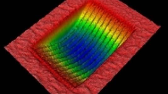
To begin to address this issue, the team’s new nano-mechanical plasmon modulator consists of 11 deformable micron-size gold bridges suspended 270 nanometers on top of another metallic gold layer. Plasmons, created by a laser in the upper structure of the device, travel in the air-filled gap between the gold bridges and the bottom gold layer. When a voltage is applied, the bridges are electrostatically attracted toward the bottom layer, which reduces the size of the gap under the beams, slowing down the plasmons and reducing their wavelength. This effect can be used to selectively cancel the wave, allowing the devices to be used as an optical switch.
“The beauty of nano-mechanical plasmon modulators is that they incorporate nano-electro-mechanical-systems (NEMS) to precisely deform the path of a propagating plasmon,” said Daniel López, a scientist at the Center for Nanoscale Materials at Argonne. “Since the NEMS used in our prototype were fabricated with conventional semiconductor fabrication processes and require actuation voltages compatible with the smallest high-speed transistors, the plasmon modulator can play a unique and important role as a building block for optoelectronic integration.”
Although the prototype is approximately 23 micrometers in length, according to NIST researcher Vladimir Aksyuk, their calculations show that the device could be shortened by a factor of 10, scaling the device’s footprint down by a factor of 100. By simultaneously reducing the device’s length and the size of the gap, the group was able to maintain the device’s modulation range without affecting its performance.
“With these prototypes we showed that nano-mechanical phase tuning is efficient,” said Aksyuk. “This effect can be generalized to other tunable plasmonic devices that need to be made smaller. And as they get smaller, you can put more of them on the same chip, bringing them closer to being practical realization.”
Small enough to serve in existing and future computer and communication architectures, this technology may also enable electrically tunable and switchable thin optical components that can be integrated into semiconductor devices using commercial semiconductor manufacturing processes.
B.S. Dennis, M.I. Haftel, D.A. Czaplewski, D. Lopez, G. Blumberg and V.A. Aksyuk. “Compact Nano-Mechanical Plasmonic Phase Modulators.” Nature Photonics.