
ARGONNE, Ill. – By pairing the capabilities of X-ray analysis and extremely precise microscopy, scientists at the U.S. Department of Energy’s Argonne National Laboratory have developed a way to simultaneously determine the physical structure and chemical makeup of materials at close to the atomic level. The research opens new routes to the next generation of materials for a wide assortment of energy-related applications.
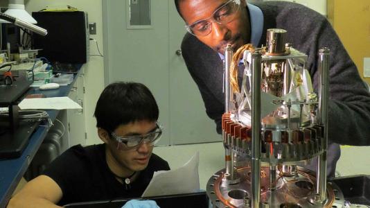
Since its Nobel Prize-winning invention in the 1980s, scanning tunneling microscopy (STM) has let researchers view an immense range of different materials at the atomic level. STM offers a finer degree of spatial resolution than virtually any other imaging technique, although it has one significant drawback, said Argonne nanoscientist Volker Rose.
“STM was an incredible breakthrough when it was discovered, but the problem with it is that even though we can basically see where all the atoms are, it doesn’t provide direct information about the chemistry or the magnetic properties,” Rose said.
Overcoming this “chemical blindness” while keeping the ability to study materials at such a small scale has proved challenging for the scientific community, but by combining the resources offered by Argonne’s Advanced Photon Source, Center for Nanoscale Materials and Electron Microscopy Center, one of Rose’s recent studies blazes a path forward.
In the recently published study, Rose and his team report on a new technique, called “synchrotron X-ray scanning tunneling microscopy,” which unites STM with the synchrotron X-rays provided by the Advanced Photon Source. The team used a tiny copper sample to determine the limitations and opportunities of the technique. Alone, the synchrotron cannot achieve the spatial resolution that STM offers, but jointly they provide the quality and type of data the researchers looked for.
“One can think about our scientific abilities as similar to the abilities of an athlete who is good at multiple sports,” Rose said. “A baseball player might not be terrific at soccer, or vice versa, because the requirements for each are different. But having a person—or in our case, an experimental technique—that combines the power of multiple approaches will have a lasting impact and hopefully accelerate the development of a number of new technologies.
“Currently, each tool is used by a different scientific community, but this is a great example of when combined expertise can really speed discovery,” he added.
Because synchrotron X-ray scanning tunneling microscopy could be used to investigate a vast array of different materials, Rose believes that the technique will help scientists and engineers develop new generations of catalysts, nanoscale magnetic systems and solar cells. “With catalysis, having this degree of resolution will show us where the active sites are on individual catalysts, and we can see exactly how the reaction occurs,” he said. “With solar cells, we can get a much better view of the surface impurities that currently reduce their efficiencies.”
Rose anticipates that the new technique will ultimately be able to study the electronic, chemical and magnetic properties of individual atoms.
Funding for the research was provided by the U.S. Department of Energy’s Office of Science through an Early Career Award that Rose received in 2012.
An article based on the study, “Synchrotron X-Ray Scanning Tunneling Microscopy: Fingerprinting Near to Far Field Transitions on Cu(111) Induced by Synchrotron Radiation,” appears in the May 28 issue of Advanced Functional Materials.
Argonne National Laboratory seeks solutions to pressing national problems in science and technology. The nation’s first national laboratory, Argonne conducts leading-edge basic and applied scientific research in virtually every scientific discipline. Argonne researchers work closely with researchers from hundreds of companies, universities, and federal, state and municipal agencies to help them solve their specific problems, advance America’s scientific leadership and prepare the nation for a better future. With employees from more than 60 nations, Argonne is managed by UChicago Argonne, LLC for the U.S. Department of Energy’s Office of Science.
The Advanced Photon Source at Argonne National Laboratory is one of five national synchrotron radiation light sources supported by the U.S. Department of Energy’s Office of Science to carry out applied and basic research to understand, predict, and ultimately control matter and energy at the electronic, atomic, and molecular levels, provide the foundations for new energy technologies, and support DOE missions in energy, environment, and national security. To learn more about the Office of Science X-ray user facilities, click here.
The Center for Nanoscale Materials at Argonne National Laboratory is one of the five DOE Nanoscale Science Research Centers (NSRCs), premier national user facilities for interdisciplinary research at the nanoscale, supported by the DOE Office of Science. Together the NSRCs comprise a suite of complementary facilities that provide researchers with state-of-the-art capabilities to fabricate, process, characterize and model nanoscale materials, and constitute the largest infrastructure investment of the National Nanotechnology Initiative. The NSRCs are located at DOE’s Argonne, Brookhaven, Lawrence Berkeley, Oak Ridge and Sandia and Los Alamos National Laboratories. More information about the DOE NSRCs is available online.
The Electron Microscopy Center (EMC) at Argonne National Laboratory develops and maintains unique capabilities for electron beam characterization and applies those capabilities to solve materials problems. The EMC staff carry out research with collaborators and users from Argonne, universities, and other laboratories. The expertise and facilities of the EMC additionally serve a group of national and international researchers. The EMC emphasizes three major areas: materials research, technique and instrumentation development, and operation as a national research facility. The EMC is supported by the DOE Office of Science. For more information, please visit http://www.msd.anl.gov/groups/emc/.
DOE’s Office of Science is the single largest supporter of basic research in the physical sciences in the United States, and is working to address some of the most pressing challenges of our time.