![Fig. 2. (a) Field dependent conductance at elevated temperatures. The cusp shape curve at 1.6 K can be fitted with the 2D Hikami-Larkin-Nagaoka equation, (b) WAL of [Pb2BiS3][AuTe2] resembles that of Bi and TI Bi2Te3. The temperature is 2 K.](/sites/www/files/171362_SH2_high-mobility-Picture2.png)
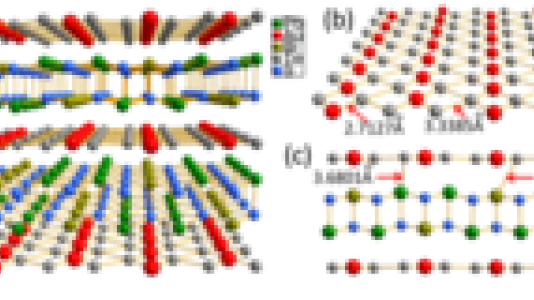
We studied the two-dimensional (2D) compound [Pb2BiS3][AuTe2], which is a natural hetero structure of two different layers. The structure is composed of stacking layers of weakly coupled [Pb2BiS3]1+ and [AuTe2]1- sheets, Fig.1. The insulating [Pb2BiS3]1+ sheet inhibits interlayer charge hopping and confines the carriers in the basal plane of the single-atom-thick conducting [AuTe2]1- layer. Magneto-transport measurements and theoretical calculations show that [Pb2BiS3][AuTe2] is a multiband semimetal with a compensated density of electrons and holes, which exhibits a high hole carrier mobility of ∼1,360 cm2/(V/s). This material possesses an extremely large anisotropy, G = ρc/ρab ≈ 104, comparable to those of the benchmark 2D materials graphite and Bi2Sr2CaCu2O6+δ. The electronic structure features linear band dispersion at the Fermi level and ultrahigh Fermi velocities of 106 m/s, which are virtually identical to those of graphene. Our results provide a novel candidate for a monolayer platform to investigate emerging electronic properties. One example of this is the presence of large spin-orbit coupling and helical spin textures.
This compound also exhibits novel quantum phenomena because of the strong spin-orbit coupling (SOC), Fig. 2(a). In comparison of conductance with the topological insulator (TI) Bi2Te3 and semi-metal Bi which are known for having strong SOC among materials systems, Fig. 2(b), the striking resemblance of [Pb2BiS3][AuTe2] and Bi2Te3 may be unusual. In order to gain a deeper understanding, we quantitatively investigated through theoretical calculations and categorize the TI material Bi2Te3 into the unconventional class of systems and the rest such as Au into the conventional class. [Pb2BiS3][AuTe2] falls between these two classes, suggesting the strong SOC, heterostructured systems may have potential for spin generation for spin-orbitronics that is currently under intense investigations to achieve tunable and large spin polarized currents. This work points out that naturally forming heterostructures made of heavy atoms provide a new direction for exploring novel quantum phenomena at the atomic scale. Given the large number of naturally formed organic and inorganic heterostructures and their hybrids, more discoveries can be expected in this direction.
“Large spin-orbit coupling and helical spin textures in 2D heterostructure [Pb2BiS3][AuTe2]” L. Fang, J. Im, W. DeGottardi, Y. Jia, A. Glatz, K. A. Matveev, W.-K. Kwok, G. W. Crabtree & M. G. Kanatzidis Scientific Reports 2016, 6, 35313. (DOI: 10.1038/srep35313)
“Two-dimensional Mineral [Pb2BiS3][AuTe2]: High mobility Charge Carriers in Single-atom-thick Layers” Fang, L.; Im, J.; Stoumpos, C.; Shi, F.; Dravid, V.; Leroux, M.; Freeman, A.; Kwok, W.-K.; Chung, D. Y.; Kanatzidis, M. J. Amer. Chem. Soc., 2014, 137, 2311-7. (DOI: 10.1021/ja5111688)