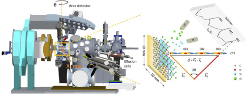
There is an emerging synthesis strategy of high-quality condensed matter materials that is poised to revolutionize the field of microelectronics. In this project, we investigated the physics of how 2D crystals grow on graphene with in situ X-ray scattering at the Advanced Photon Source. We and others have demonstrated that single-crystal thin films can be detached from the substrates on which they are grown and re-attached to another material with little to no change in defect concentration. In this way, multifunctional heterostructures can be “unzipped” and used for a wide array of applications while the high value and often exotic single-crystal substrates can be recycled.
The tremendous potential and greatest opportunity to reshape the landscape is the ability to merge high-quality dissimilar 2D crystalline materials to create novel multi-functional platforms, which has eluded the microelectronics industry for decades. In our project, we conducted in situ X-ray studies on the fundamental physics of “remote epitaxy.” The results shed new light on the process by which epitaxial growth of a thin film occurs through a graphene buffer layer from the seeding growth substrate and the key process essential to the new synthesis strategy [1,2].