Below is a comprehensive list of articles, events, projects, references and research related content that is specific to the term described above. Use the filter to narrow the results further. To explore additional science and technology topics that Argonne researchers and engineers may be working on please visit our Research Index.
This system was constructed as an alternative for detection of obscured objects and material. Depending on the geometry of the given situation a flat-panel source can be used in tomography, radiography, or tomosynthesis. Furthermore, the unit can be used as a portable electron or X-ray scanner or an integral part of an existing detection system. UNCD field emitters show great field emission output and can be deposited over large areas as the case with carbon nanotube “forest” (CNT) cathodes. Furthermore, UNCDs have better mechanical and thermal properties as compared to CNT tips which further extend the lifetime of UNCD based FEA.
The first layer is seeded with nanodiamond particles. The substrate with the first layer disposed thereon is maintained at a first temperature and a first pressure in a mixture of gases which includes nitrogen. The first layer is exposed to a microwave plasma to form a nitrogen doped ultrananocrystalline diamond film on the first layer, which has a percentage of nitrogen in the range of about 0.05 atom % to about 0.5 atom %. The field emitter has about 1012 to about 1014 emitting sites per cm2. A photocathode can also be formed similarly by forming a nitrogen doped ultrananocrystalline diamond film on a substrate similar to the field emitter, and then hydrogen terminating the film. The photocathode is responsive to near ultraviolet light as well as to visible light.
The cathode and anode are in the form of electroactive sheets separated from each other by a membrane that is permeable to the electrolyte. One or more of the cathode and anode comprises two or more layers of carbon nanotubes, one of which layers includes electrochemically active nanoparticles and/or microparticles disposed therein or deposited on the nanotubes thereof. The majority of the carbon nanotubes in each of the layers are oriented generally parallel to the layers. Optionally, one or more of the layers includes an additional carbon material such as graphene, nanoparticulate diamond, microparticulate diamond, and a combination thereof.
Nanocrystalline diamond coatings exhibit stress in nano/micro-electro mechanical systems (MEMS). Doped nanocrstalline diamond coatings exhibit increased stress. A carbide forming metal coating reduces the in-plane stress. In addition, without any metal coating, simply growing UNCD or NCD with thickness in the range of 3-4 micron also reduces in-plane stress significantly. Such coatings can be used in MEMS applications.
The mixture of gases include a source of a p-type or an n-type dopant. The plasma ball is disposed at a first distance from the diamond substrate. The diamond substrate is maintained at a first temperature. The plasma ball is maintained at the first distance from the diamond substrate for a first time, and a UNCD film, which is doped with at least one of a p-type dopant and an n-type dopant, is disposed on the diamond substrate. The doped UNCD film is patterned to define UNCD electrical contacts on the diamond substrate.
A method of forming a p-n junction device comprises providing a base layer including a p-type diamond. A monolayer or few layer of a transition metal dichalcogenide (TMDC) is disposed on at least a portion of the base layer so as to form a heterojunction therebetween. The TMDC monolayer is an n-type layer such that the heterojunction between the intrinsic and p-type diamond base layer and the n-type TMDC monolayer is a p-n junction.
The system includes graphene and graphene oxide formed by an exfoliation process or solution processing method to dispose graphene and/or graphene oxide onto a Substrate. The system further includes an opposing wear member disposed on another Substrate and a gas atmosphere of an inert gas like N2, ambient, a humid atmosphere and a water Solution.
Express Licensing
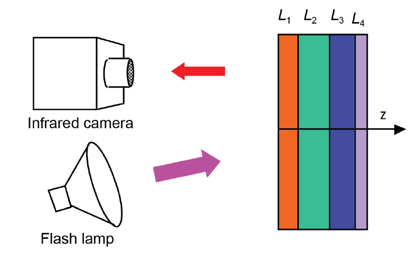
Pulsed thermal imaging is widely used for nondestructive evaluation of advanced materials and components. Thermal imaging methods to analyze single-layer materials are well developed. However, a general method for analyzing multi-layer materials and coatings/films has not been developed due to the complexity of material systems and lack of an analytical solution. This technology provides a general method, test system including a filter, and numerical algorithm for automated analysis of thermal imaging data for multi-layer coating materials.
Argonne’s pulsed thermal imaging-multilayer analysis method can accurately measure coating thermal conductivity and heat capacity (and/or thickness) distributions over an entire component’s surface. The method analyzes a temporal series of measured thermal imaging data to determine the properties for all coating layers based on a multilayer model. Argonne’s invention is currently the only method that can analyze coatings of more than one layer, is fully automated to produce 2D layer property images, and has validated high accuracy.
Argonne’s approach includes an infrared filter for flash lamps to eliminate the flash’s infrared radiation, ensuring accurate detection of surface temperature during pulsed thermal imaging tests.
Key to Argonne’s thermal multi-layer analysis method is the numerical algorithm used for automated analysis of thermal imaging data for multi-layer materials, implemented in dedicated, Argonne-created software that allows for complete data-processing automation without the need of user intervention.
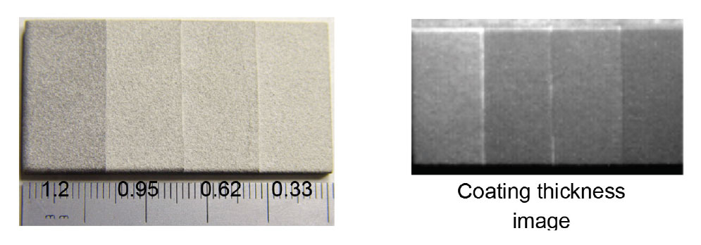
Proof of Concept: the technology has been tested and proven to work for coated engine parts.
Wide adoption of Materials by Design approaches for nanomaterials such as catalysts, energy storage materials, and new drugs has greatly increased the need for nanomaterials analysis tools.
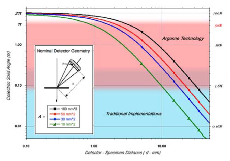
Scanning Electron Microscopes (SEMs) are widely used by materials researchers. Frequently fitted with ancillary x‐ray detectors for elemental analysis of materials, these instruments are limited in their nanoscale analytical sensitivity because they capture less than 2% of the meager x‐ray signals generated when ultra small particles and thin films are probed by the minute electron beams in today’s SEMs. To address this limitation, scientists at Argonne National Laboratory’s Electron Microscopy Center invented a new x‐ray detection system that increases the detection capability of SEMs during nanomaterials analysis.
Traditional implementations of solid state x‐ray detectors in SEMs capture only about 0.05–0.1 sR (<2%) of the signal generated, as indicated by the blue shaded region in the figure below. Argonne’s technology overcomes this limitation through an innovative new geometry and positioning of the x‐ray detection system.
For nanoparticles and thin film analysis, this invention facilitates capture of more than π steradians (sR) or ~50% of available x‐ray signal, encompassing both the blue and red regions in the figure. The technology also features a proprietary electron shield to protect the system from electrons hitting the detector and in addition, integrates electron detection to provide the enhanced capability to image the nanoparticles and thin films as well as identify their elemental composition. The Argonne system can be retrofitted onto existing SEMs or provided as an accessory detector for new SEMs.
Argonne’s π Steradian X‐Ray Detection System can substantially reduce the time and cost for conducting routine analysis of nanomaterials by increasing detection capabilities of SEMs at the nanoscale by up to 500%. It enables highresolution rapid imaging and analysis, which facilitate new discoveries and scientific understanding of nanomaterials not practical using conventional detector implementations. The new system also accelerates “materials design and discovery” by enabling effective characterization of nanostructures engineered to evoke specific functionality in a timely fashion, in sync with the modeling and synthesis steps.
The cost of the new Argonne detector system is estimated to be an incremental addition to the cost of a traditional detector.
Scientists at Argonne National Laboratory have created a stable, non-reactive nanofluid that exhibits enhanced heat-transfer properties with only a minimal increase in pumping power required relative to the base-heat transfer fluid.
Nanofluids—liquid mixtures with a small concentration of nanoparticles in suspension—have unique properties that make them potentially useful for heat transfer. The study of nanofluid heat transfer is a relatively new area of scientific exploration, and although industrial applications for nanofluid technology are still in their infancy, some mixtures have been shown to substantially increase the heat-transfer characteristics of the nanofluid over the base liquid.
Argonne’s nanofluid is composed of ceramic nanoparticles suspended in a base-heat-transfer fluid made up of water and water/ethylene glycol mixtures. Ceramic nanoparticles are not susceptible to surface oxidation, and enjoy significantly better chemical stability over longer periods of time than metals. Although ceramics generally have low thermal conductivity, some ceramics have properties that make them attractive candidates for use in nanofluids for commercial and industrial heat-transfer applications.
Proof of concept