Scientific Achievement
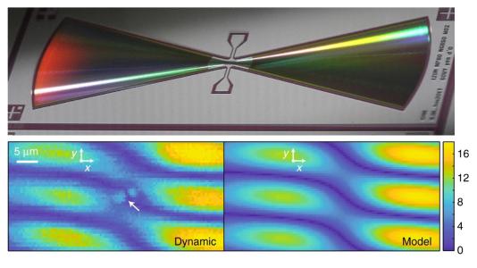
Dynamic strain was found to correlate with enhanced photoluminescence from optically active point defects used for solid-state qubits in 4H-SiC. Point defects in silicon carbide couple to strain, which can be used to tune the defect properties and coherently control spin states. Here the authors fabricate Gaussian-shaped surface acoustic wave transducers, develop a stroboscopic x-ray imaging method to measure dynamic lattice curvature, and observe its effects on the defect photoluminescence. Control of local lattice perturbations near optically-active defects in semiconductors is a key step to harnessing the potential of solid-state qubits for quantum information science and nanoscale sensing. The development of a stroboscopic scanning X-ray diffraction microscopy approach is reported for real-space imaging of dynamic strain used in correlation with microscopic photoluminescence measurements. This technique was demonstrated in 4H-SiC, which hosts long-lifetime room temperature vacancy spin defects. Using nano-focused X-ray photon pulses synchronized to a surface acoustic wave launcher, an effective time resolution of ~100 ps was achieved at a 25 nm spatial resolution to map micro-radian dynamic lattice curvatures. The acoustically induced lattice distortions near an engineered scattering structure are correlated with enhanced photoluminescence responses of optically-active SiC quantum defects driven by local piezoelectric effects.
Significance and Impact
Combining time-resolved optical and X-ray microscopy demonstrates a unique route for quantifying dynamic structure-function relationships in operando quantum materials. These results demonstrate a unique route for directly imaging local strain in nanomechanical structures and quantifying dynamic structure-function relationships in materials under realistic operating conditions.
Research Details
- Fabricated Gaussian-shaped piezoelectric transducers were used to drive focused 350 MHz surface acoustic waves in 4H-SiC.
- A stroboscopic X-ray diffraction microscopy method was developed to directly image local lattice dynamics, quantifying their effect on defect photoluminescence.
Work was performed in part at the Center for Nanoscale Materials and Advanced Photon Source.
About Argonne’s Center for Nanoscale Materials
The Center for Nanoscale Materials is one of the five DOE Nanoscale Science Research Centers, premier national user facilities for interdisciplinary research at the nanoscale supported by the DOE Office of Science. Together the NSRCs comprise a suite of complementary facilities that provide researchers with state-of-the-art capabilities to fabricate, process, characterize and model nanoscale materials, and constitute the largest infrastructure investment of the National Nanotechnology Initiative. The NSRCs are located at DOE’s Argonne, Brookhaven, Lawrence Berkeley, Oak Ridge, Sandia and Los Alamos National Laboratories. For more information about the DOE NSRCs, please visit https://science.osti.gov/User-Facilities/User-Facilities-at-a-Glance.
About the Advanced Photon Source
The U. S. Department of Energy Office of Science’s Advanced Photon Source (APS) at Argonne National Laboratory is one of the world’s most productive X-ray light source facilities. The APS provides high-brightness X-ray beams to a diverse community of researchers in materials science, chemistry, condensed matter physics, the life and environmental sciences, and applied research. These X-rays are ideally suited for explorations of materials and biological structures; elemental distribution; chemical, magnetic, electronic states; and a wide range of technologically important engineering systems from batteries to fuel injector sprays, all of which are the foundations of our nation’s economic, technological, and physical well-being. Each year, more than 5,000 researchers use the APS to produce over 2,000 publications detailing impactful discoveries, and solve more vital biological protein structures than users of any other X-ray light source research facility. APS scientists and engineers innovate technology that is at the heart of advancing accelerator and light-source operations. This includes the insertion devices that produce extreme-brightness X-rays prized by researchers, lenses that focus the X-rays down to a few nanometers, instrumentation that maximizes the way the X-rays interact with samples being studied, and software that gathers and manages the massive quantity of data resulting from discovery research at the APS.
This research used resources of the Advanced Photon Source, a U.S. DOE Office of Science User Facility operated for the DOE Office of Science by Argonne National Laboratory under Contract No. DE-AC02-06CH11357.
Argonne National Laboratory seeks solutions to pressing national problems in science and technology. The nation’s first national laboratory, Argonne conducts leading-edge basic and applied scientific research in virtually every scientific discipline. Argonne researchers work closely with researchers from hundreds of companies, universities, and federal, state and municipal agencies to help them solve their specific problems, advance America’s scientific leadership and prepare the nation for a better future. With employees from more than 60 nations, Argonne is managed by UChicago Argonne, LLC for the U.S. Department of Energy’s Office of Science.
The U.S. Department of Energy’s Office of Science is the single largest supporter of basic research in the physical sciences in the United States and is working to address some of the most pressing challenges of our time. For more information, visit https://energy.gov/science.