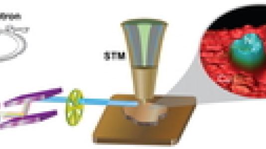
By using synchrotron X-rays as a probe and a nanofabricated smart tip of a tunneling microscope as a detector, the chemical fingerprinting of individual nickel clusters on a Cu(111) surface was achieved at 2 nm lateral resolution, and at the ultimate single-atomic height sensitivity. Moreover, by varying the photon energy, local photoionization cross sections of just a single Ni nanocluster was successfully measured, which opens new exciting opportunities for chemical imaging of nanoscale materials.
A team of researchers from Argonne’s Center for Nanoscale Materials and Advanced Photon Source, and Ohio University, devised a technique that simultaneously resolves the chemical characterization and topography of nanoscale materials down to single atom height sensitivity. The technique combines synchrotron X-rays (SX) and scanning tunneling microscopy (STM). In experiments, SX was used as a probe and a nanofabricated smart tip of a STM was used as a detector. Also, photoionization cross-sections of a single-nickel nanocluster were measured by varying the photon energy – opening the door to new opportunities for chemical imaging of nanoscale materials. Until now, a spatial limit of about only 10 nm was attainable and photoionization cross-sections could only be obtained as an average over a large sample area.
N. Shirato, M. Cummings, H. Kersell, Y. Li, B. Stripe, D. Rosenmann, S.-W. Hla, V. Rose, Nano Lett., 2014, 14, 6499.
In The News