This proposal focuses on the development of a warm radio-frequency electronic readout and control (RF-R&C) to achieve quantum error correction (QEC) of a large quantum correction. Development of this dynamic modular system will focus on the following topics:
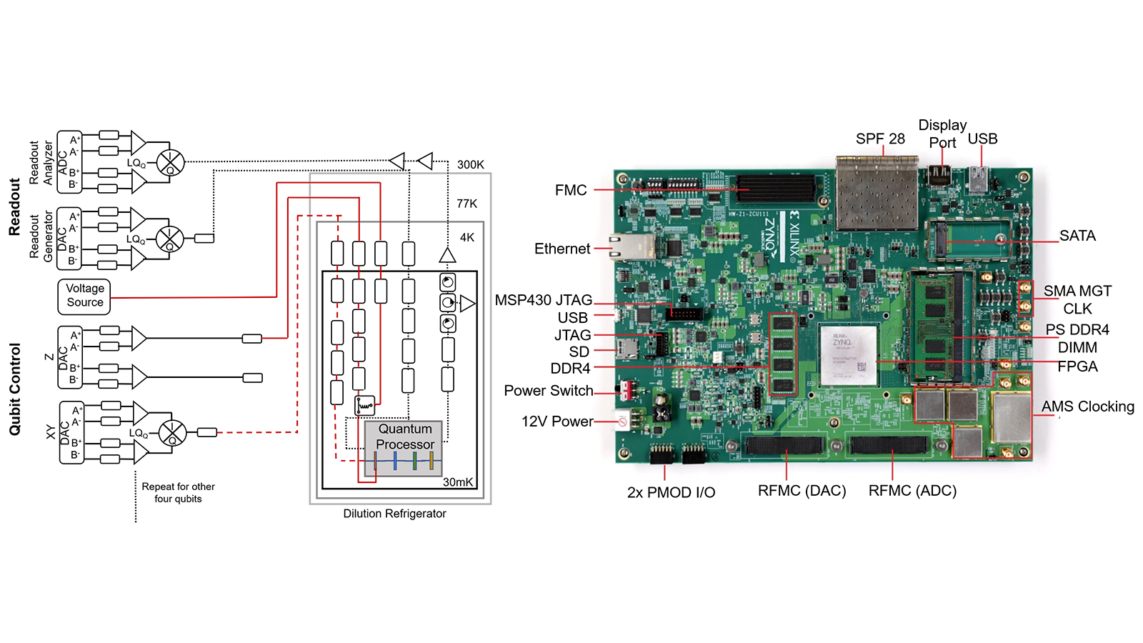
A quantum correction program is made of sequential control pulses applied to the inputs. As in a standard computer program, most useful quantum correction programs require conditional branching. Hence, qubit readout and control systems must prioritize hardware latency, fast qubit state detection and control. The readout must be connected to the control of the qubits in a tight feedback loop. To perform those functions, we will use ultra-fast field-programmable gate arrays (FPGAs), analog-to-digital converters (ADCs) and digital-to-analog converters (DACs). The hardware platform is based on the Xilinx ZCU111. We will develop readout and control tools fully utilizing the resources of the hardware. The ZCU111 has been developed around the Xilinx XC7ZU28 FPGA. This FPGA incorporates eight 12-bit ADCs running at 4 Gs/s and eight DACs running at 6.5 Gs/s. The roundtrip latency, including the ADC, DAC and logic interfaces, has been measured to be 100 ns, making possible total latencies of less than 200 ns for feedback control. The FPGA also has about 1 million logic gates, half a million logic blocks and 70 Mb of internal memory. All that functionality combined with more than 4,000 digital signal processors will allow the implementation of complex QEC algorithms.
We will also develop the appropriate RF hardware to interface to test qubit systems. The qubits will be supplied by our collaborators. The number of qubits to be controlled by the electronics will incrementally increase. A ZCU111 board can control up to seven qubits. The design easily scales to a larger system by using more boards.