Instrumentation

Argonne maintains a wide-ranging science and technology portfolio that seeks to address complex challenges in interdisciplinary and innovative ways. Below is a list of all articles, highlights, profiles, projects, and organizations related specifically to instrumentation.

Filter Results

  • SDN Multiple Operating System Rotational Environment (SMORE) utilizes software defined networking (SDN) to programmatically switch the flow of packets from users to a given set of servers. By periodically switching which servers respond to user requests.
    Intellectual Property Available to License

    Cybersecurity issues are a day-to-day struggle for businesses and organizations. Keeping information secure can be a herculean task. SMORE-MTD, developed by Argonne’s Joshua Lyle and Nate Evans with laboratory funding, defends against cybersecurity attacks by using software-defined networking to manipulate network paths that service user requests.

    By randomly selecting which server and service will respond to a given user’s request, SMORE-MTD makes it more difficult for an attacker to identify which services to attack. SMORE-MTD also increases organizations’ resilience by preventing an attacker exploit from being routed to the vulnerable software, forcing attackers into repeated attacks that are more likely to be noticed. SMORE-MTD also eliminates the need to install and maintain configuration software on each host in rotation, which reduces complexity and increases the amount of software available for use.
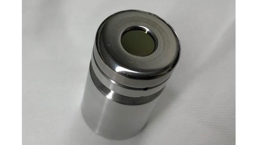
  • This invention describes a holder that was specifically designed to hold a mesh and sample solution in a simple, reliable, cost effective, and user-friendly way.
    Intellectual Property Available to License
    US Patent 16/903,601
    • 3D Printed Mesh Holder for Serial Crystallography (IN-19-083)

    The invention describes a new sample holder for serial crystallography that utilizes a magnetic compression ring to immobilize sample fluids between mesh. Advantages of the new technology include, compatibility with standard single crystallography mounting equipment, 3D printable, minimal assembly required, high reusability, and cost effective.                                 

  • This invention is a new method of fabricating concave/convex optics in which a singlestructure crystal wafer will undergo curvature due to forces created by vacuum rather than the standard compressive techniques.
    Intellectual Property Available to License
    US Patent 8,557,149
    • System and method for implementing enhanced optics fabrication

    This method attempts to reduce the amount of residual stress and aberration that occurs by eliminating the forceful bending of such standard devices. This invention solves a difficult problem faced by those wishing to create a crystal surface, with even modest curvature, without causing non-uniform residual surface stresses.

  • Method to characterize nanofiber assemblies from images
    Intellectual Property Available to License

    US Patent 9,639,926 B1
    • Image processing tool for automatic feature recognition and quantification

    A system for defining structures within an image is described. The system includes reading of an input file, preprocessing the input file while preserving metadata such as scale information and then detecting features of the input file. In one version the detection first uses an edge detector followed by identification of features using a Hough transform. The output of the process is identified elements within the image.

  • A high-resolution, active-optic X-ray fluorescence analyzer combining a large acceptance solid angle with wide energy tunability
    Intellectual Property Available to License
    US Patent 8,130,902B2
    • High-Resolution, Active-Optic X-Ray Fluorescence Analyzer (IN-06-085)

    Active optics apparatus and method for aligning active optics are provided for a high-resolution, active optic fluorescence analyzer combining a large acceptance solid angle with wide energy tunability. A plurality of rows of correctors selectively controlled to bend an elongated strip of single crystal material like Si (400) into substantially any precisely defined shape. A pair of pushers engages opposite ends of the silicon crystal strip exert only a force along the long axis of the crystal strip, and does not induce additional bending moments which would result in a torsion of the crystal.

  • A method to fabricate dielectric capacitors with increased capacitance and durability that can boost the capability of power electronics.
    Intellectual Property Available to License

    US Patent 9,646,766 B2
    • Method of making dielectric capacitors with increased dielectric breakdown strength (IN-10-096)

    The invention is directed to a process for making a dielectric ceramic film capacitor and the ceramic dielectric laminated capacitor formed therefrom, the dielectric ceramic film capacitors having increased dielectric breakdown strength. The invention increases breakdown strength by embedding a conductive oxide layer between electrode layers within the dielectric layer of the capacitors. The conductive oxide layer redistributes and dissipates charge, thus mitigating charge concentration and micro fractures formed within the dielectric by electric fields.