
Manufacturing Engineering

Argonne maintains a wide-ranging science and technology portfolio that seeks to address complex challenges in interdisciplinary and innovative ways. Below is a list of all articles, highlights, profiles, projects, and organizations related specifically to manufacturing engineering.

Filter Results

  • Advanced Materials Manufacturing

    Argonne’s Advanced Materials Manufacturing work focuses on research, development and demonstration of new materials with desirable properties for use in energy saving applications, such as advanced batteries and catalysts.
  • Work with Us

    Argonne works with industry partners to solve their enduring manufacturing R&D challenges, identify commercialization opportunities, license new technologies and introduce transformational discoveries to the marketplace.
  • Process for preparing lower-cost, high-throughput multiple patterning photolithography
    Intellectual Property Available to License
    US Patent 9,684,234
    • Sequential Infiltration Synthesis for Enhancing Multiple Patterning Lithography (ANL-IN-12-107 and ANL-IN-12-107B)

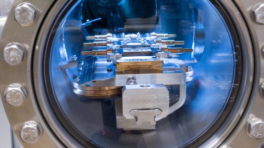
    Technology available for licensing: The invention is simplified methods of multiple-patterning photolithography using sequential infiltration synthesis (SIS) to modify the photoresist such that it withstands plasma etching better than unmodified resist and replaces one or more hard masks and/or a freezing step in MPL processes including litho-etch-litho-etch photolithography or litho-freeze-litho-etch photolithography. Potential applications of these methods and system extend to virtually all technologies in which periodic nanomaterial structures are desirable, including optoelectronics, sensors, membranes, photonic crystals, dielectric materials, and electronics.

    Benefits

    • Process for preparing lower-cost, high-throughput multiple patterning photolithography.
    • Can increase the plasma etch resistance and/or render a photoresist layer insoluble in photoresist solvents, thus obviating the need for one or more steps of present techniques of multiple-patterning lithography.
    • Utilizes alternating exposures to gas phase precursors that infiltrate the organic or partially organic resist material to form a protective component within the resist layer, modifying the standard multiple-patterning lithography techniques to reduce the number of steps and/or decrease the cost and time that these techniques presently require
  • Plasma etch resist material modified by an inorganic protective component via sequential infiltration synthesis (SIS) and methods of preparing the modified resist material
    Intellectual Property Available to License
    US Patent 9,786,511
    • Sequential Infiltration Synthesis for Enhancing Advanced Lithography (ANL-IN-10-106B)

    Technology available for licensing: The SIS process forms the protective component within the bulk resist material through a plurality of alternating exposures to gas phase precursors which infiltrate the resist material.

    Benefits

    • The plasma etch resist material may be initially patterned using photolithography, electron-beam lithography or a block copolymer self-assembly process.
    • The modified resist material is characterized by an improved resistance to a plasma etching or related process relative to the unmodified resist material, and
    • Thereby allowing formation of patterned features into a substrate material, which may be high-aspect ratio features.
  • A method of preparing tunable inorganic patterned nanofeatures by infiltration of a block copolymer scaffold having a plurality of self-assembled periodic polymer microdomains
    Intellectual Property Available to License
    Ordered nanoscale domains by infiltration of block copolymers
    • ANL-IN-10-017 entitled Ordered nanoscale domains by infiltration of block copolymers”

    The method may use sequential infiltration synthesis (SIS), related to atomic layer deposition (ALD).

    Benefits

    • Tunable inorganic features can be selectively formed on the microdomain to form a hybrid organic/inorganic composite material of the metal precursor and a co-reactant.
    • The organic component may be optionally removed to obtain inorganic features with patterned nanostructures defined by the configuration of the microdomain.