The CNM’s ability to fabricate complex nanostructures and devices is based on the advanced tool set housed within the Nanofabrication and Devices group’s clean room. The clean room staff have extensive expertise in the synthesis, fabrication, and processing of nanomaterials and the design and development of nanodevices, including manufacturing of micro/nano-electro-mechanical systems. They provide not only technical expertise and training but also user support. The clean room spans over 18,000 square feet and contains a remarkable depth and breadth of nanofabrication equipment. See below for the major equipment list.
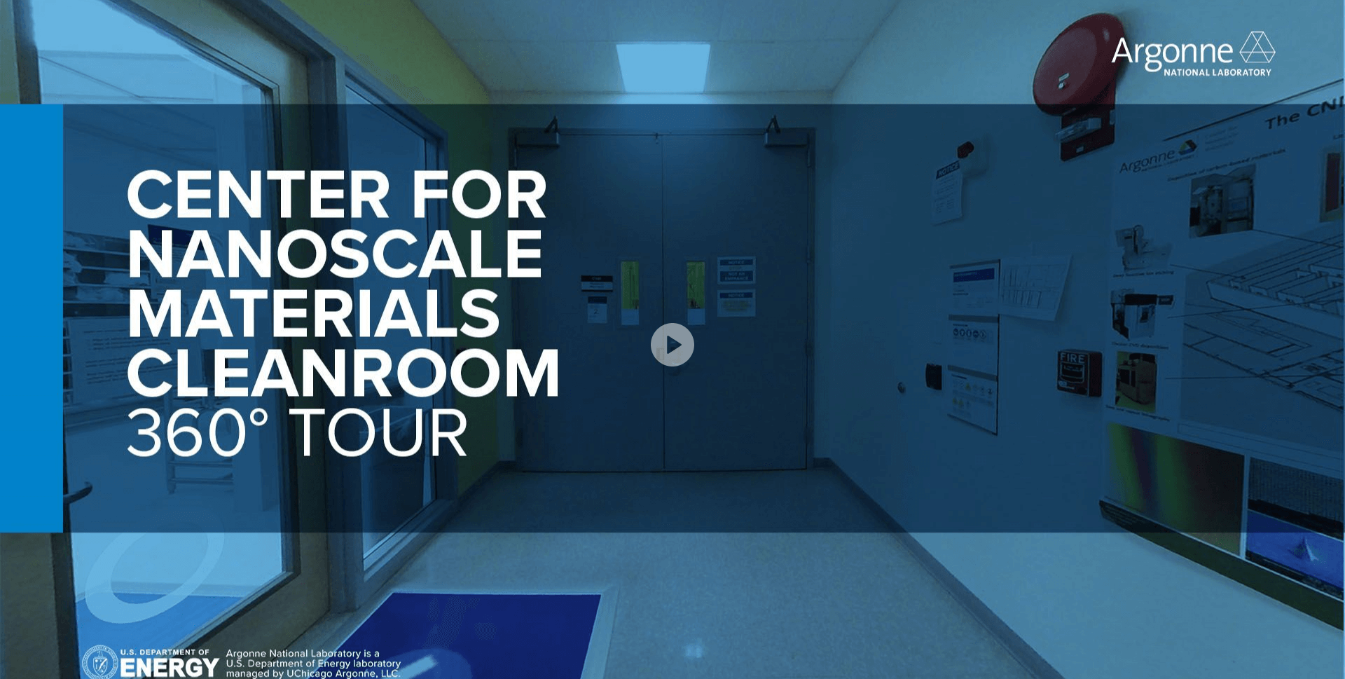
Virtual 360° tour of the CNM cleanroom
The CNM cleanroom features unique, state-of-the-art toolsets for the creation of devices at the nanoscale. Scientists from around the world use fabrication tools and other capabilities in the cleanroom to invent new technologies and explore the evolution of the universe.
The CNM lithography suite is housed in three bays and includes several advanced lithography tools covering electron beam lithography, ion beam lithography, direct write optical lithography, contact printing with back-side alignment, nanoimprint lithography, and holographic lithography. A deposition suite, also housed in three bays, allows synthesis of a variety of materials, including metal, dielectric, and complex oxides using multi-chamber sputtering tools, electron beam evaporation, and plasma-enhanced chemical vapor deposition (PECVD). A unique synthesis tool includes microwave plasma CVD for the synthesis of diamond films
A wet etch bay includes electroplating, an electrochemical workstation, and supercritical drying capability for post-processing. The main tools in the dry etch bay are a dual chamber Oxford Instruments Plasmalab 100 and two tabletop March Plasma RIE tools. There are additional metrology tools for measurements of film thickness, critical dimensions, and stress, including profilometers, a spectroscopic ellipsometer, and atomic force microscope, as well as sample/wafer processing tools, including a critical point dryer and a cleaving machine.
Lithography
- Electron Beam Lithography System: JEOL8100FS
- Electron Beam Lithography System: Raith 150
- Focused Ion Beam: FEI Nova 600NanoLab
- Interferometric Lithography System
- Heidelberg MLA150 Maskless Lithography with 405 nm and 375 nm diodes and backside alignment
- Laser Pattern Generator: Microtech LW405
- SUSS MA6/BA6: Contact aligner for front side and front-to-back side alignment
- Wafer priming and image reversal ovens: YES-TA series
- Stepper: ASMLPAS5000wafer stepper and scanner (resolution to 500 nm; users need to supply their own 5x5 mask with standard ASML stepper marks) - 150 mm wafers
Ultralow Temperature/Strong Magnetic Field Measurements ( Quantum Devices and ADR Lab)
- BlueFors LD400 Dilution Refrigerator System: <10 mK base temperature, 5x free-space optical access points, 100x dc lines, 20x microwave lines, 2x high-pressure fill lines, expedited sample loading mechanism, low-noise RF amplifiers for qubit research
- AMI Superconductor Vector Magnet: 5T in z-axis, 1T in y-axis, 1T in x-axis, 10 mG field stability, 3-axis persistent switches
- Adiabatic Demagnetization Refrigerator (ADR) System: <60 mK base temperature, 24x dc wires, 4x superconducting microwave lines, low-noise RF amplifiers, 5T superconducting magnet
Deposition
- AJA Oxide Sputtering, 3-inch targets
- AJA Oxide Sputtering, 2-inch targets
- AJA Dielectric Sputtering
- AJA Metal Sputtering
- Atomic Layer Deposition (Arradiance Gemstar)
- Lambda Microwave Plasma CVD System: nanocrystalline diamond deposition
- Oxford Plasmalab 100 Inductively Coupled Plasma Enhanced Chemical Vapor Deposition
- Applied Materials P5000: TEOS, SiO2, SiNx, a-Si depositions
- Temescal FC2000 Electron Beam Evaporator (materials requested require process custodian approval)
- Angstrom Thermal evaporator
- Angstrom sputtering system
Dry Etching
- PlasmaTherm Versaline DSE-III Deep Reactive Ion Etcher
- RIE Oxford PlasmaLab 100, Chlorine Chamber for up to 4-inch wafers
- RIE Oxford PlasmaLab 100, Fluorine Chamber for up to 4-inch wafers
- RIE March CS-1701, Chlorine Chamber
- RIE March CS-1701, Fluorine Chamber
- RIE Oxford ICP Etcher (for up to 6-inch wafers)
- RIE Oxford ICP Etcher with ALE kit (for up to 6-inch wafers).
- Hydrofluoric (HF) vapor etcher
- Xactix X4 xenon difluoride etcher
- ESI plasma asher
Wet Chemistry
- Electroplating (Au, Cu, Fe, Ni, Pt, Bi)
- Selective wet chemical etching
- Class One rinse dryer
- CEE spin-coating and developing bench
- JST liftoff bench
Inspection and Metrology
- Bruker FastScan Atomic Force Microscope
- Filmetrics f40 thin film analyzer
- R50 Resistance Mapper
- Laser Confocal Microscope OLS4100
- Keyence Confocal Microscope
- Optical Microscopes: Olympus MX-61, MX-63
- Three-Dimensional Contact Profilometers: Dektak 8, Tencor P7
- UVISEL Spectroscopic Ellipsometer: Horiba Jobin Yvon
- Scanning Electron Microscope VEGA 3 (tungsten filament)
Post-Processing
- AS-One 150 Rapid Thermal Processor
- Cleaving Machine: LatticeGear LatticeAx 420
- Critical Point Dryer (Leica CPD300)
- ADT 7200 Dicing Saw
Piezo-Optomechanical Spectrometer (POMS)
Wear/Friction Measurements
- Multifunctional Tribometer with controlled environments
- Sonotek Ultrasonic Spray Coating System
- PI-95 in-situ TEM PicoIndenter for Nanomechanical and Nanotribological measurements
Theory
- Would you like Theory with that? Joint experimental-theory proposals are possible and encouraged; visit the Theory & Modeling group’s webpage for more information about their capabilities.